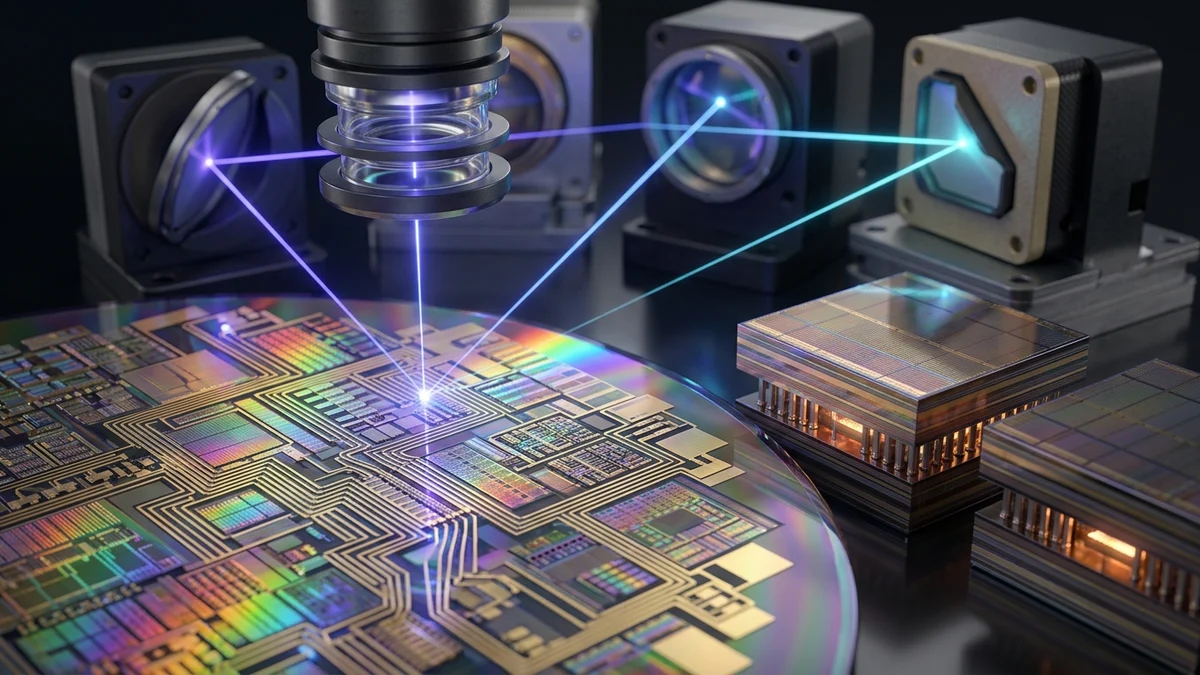
Every time you load a local language model, compile a kernel, or open a browser tab, billions of microscopic capacitors are charging and refreshing inside your system's DRAM. Yet most builders rarely see what it takes to turn raw sand into a stick of DDR5—or why AI data centers have reshaped memory pricing across the entire PC market.
From molten silicon to microscopic capacitor cells
Memory manufacturing starts with purified polysilicon melted into single-crystal cylindrical ingots, sliced into mirror-smooth wafers. Inside a cleanroom fab, photolithography and etching build repeating grids of 1T1C cells—one tiny transistor paired with one deep-trench or stacked capacitor that holds a single bit of charge. Because DRAM capacitors leak charge continuously, every cell must be refreshed thousands of times per second.
Samsung Semiconductor's official explainer walks through how individual DRAM dies are organized into chips, packages, and modules, while Crucial and Micron's factory tour shows the 34-stage probing, thinning, and validation pipeline before a module ever ships.
Why AI data centers raised the cost of memory
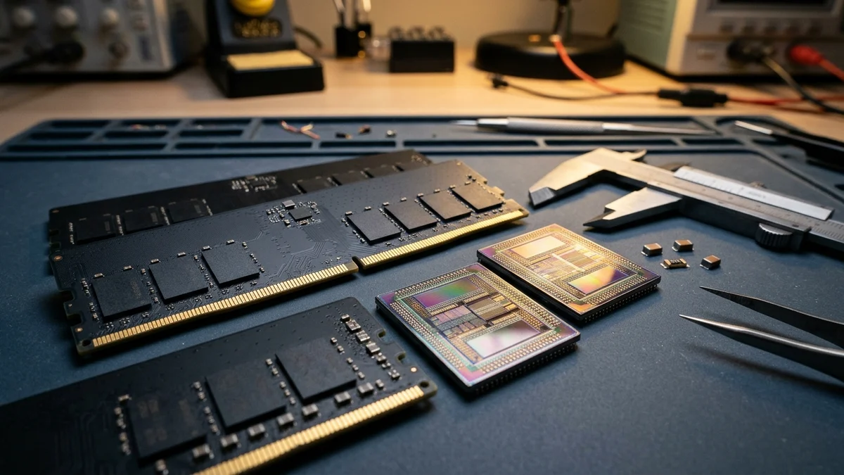
The biggest shift in modern memory economics is High Bandwidth Memory (HBM). Instead of laying dies flat on a standard DIMM stick, HBM stacks multiple DRAM dies vertically and connects them with thousands of through-silicon vias (TSVs) right beside an AI accelerator GPU. Because HBM consumes more wafer area per gigabyte and requires complex advanced packaging with lower yields, every fab line shifted toward HBM3E/HBM4 leaves fewer wafers for everyday DDR5 and LPDDR5.
What it means for local AI builders
For people running quantized models on home workstations, memory bandwidth and capacity—not just GPU cores—are the real bottleneck. Understanding how DRAM wafers are allocated explains why 64 GB and 128 GB kits carry a steep premium during AI buildouts, and why unified-memory mini-PCs and aggressive 4-bit quantization remain practical equalizers.
Original AiBrainWorX & OpenSourceCoder editorial feature published November 16, 2026.