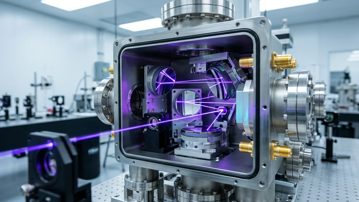
Every modern AI accelerator and high-density memory die begins as an exercise in extreme-precision light. Before a model ever runs a single token, chipmakers have to print billions of transistors onto silicon wafers using Extreme Ultraviolet (EUV) lithography at a wavelength of just 13.5 nanometers.
Tin droplets, lasers, and mirrors in a vacuum
Unlike older deep-ultraviolet scanners that shine light through glass lenses, EUV light is absorbed by almost every material—including air and glass. Inside a high-vacuum chamber, an EUV system fires a high-power CO2 laser at microscopic falling droplets of molten tin tens of thousands of times per second, turning them into plasma that emits 13.5 nm light. Multi-layer Bragg mirrors then bounce that light onto a patterned mask and down onto the silicon wafer.
ASML's official technical video walks through how a High-NA EUV system generates and shapes that light inside the machine.
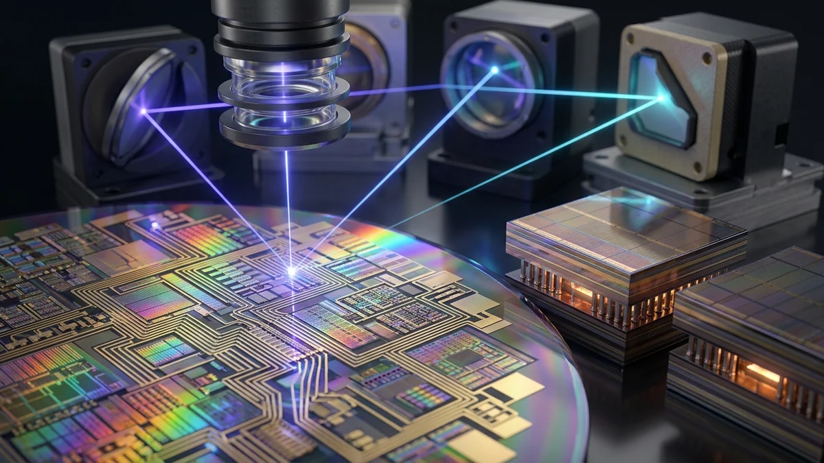
Why supply stays concentrated
Each EUV scanner costs hundreds of millions of dollars, requires specialized cleanrooms, and consumes megawatts of facility power. That physical bottleneck—more than any software layer—is why global AI compute capacity scales in multi-year fab cycles rather than overnight.
Original AiBrainWorX long-form editorial feature published November 16, 2026.